Problem Set 9#
Source: Problem_Set_9_Digital_Logic Revision: n/a
1#
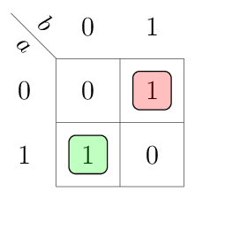
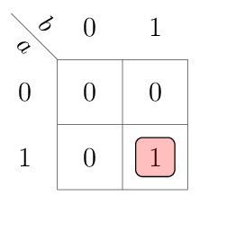
Sketch a block diagram for a magnitude comparator bit-slice circuit. Create K-maps to define the bit-slice circuit, and use them to find optimal logic equations. Sketch the bit-slice circuit.
The exercise asks for
a block diagram for a single bit slice,
K-maps for creating Boolean equations
a circuit diagram for a single bit slice
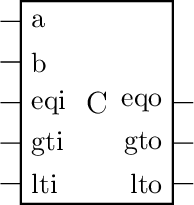
Fig. 2 Block diagram for a single bit-slice.
These bit slices are typically cascaded. For example a 4 bit comparator is interconnected as follows:
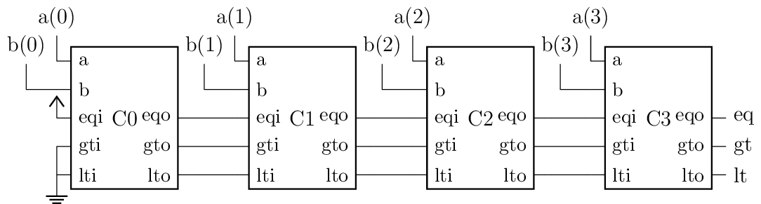
Fig. 3 Block diagram for a 4 bit comparator. a and b are the compared numbers; eq, gt, lt are inputs and outputs.
Only one of the bit slice output signals \(eq\), \(gt\) and \(lt\) can be active at the same moment, in other words these are mutually exclusive. By using this property, we can simplify the table as follows.
Note that we only write the minterms to save space.
\(a\) |
\(b\) |
\(eqi\), \(gti\), \(lti\) |
\(eqo\), \(gto\), \(lto\) |
remarks |
|---|---|---|---|---|
0 |
0 |
\(eqi = 1\) |
\(eqo = 1\) |
|
0 |
1 |
\(lto = 1\) |
don’t care about \(eqi\) |
|
1 |
0 |
\(gto = 1\) |
don’t care about \(eqi\) |
|
1 |
1 |
\(eqo = 1\) |
||
— |
— |
————— |
————— |
— |
0 |
0 |
gti = 1 |
\(gto = 1\) |
|
0 |
1 |
\(lto = 1\) |
don’t care about \(gti\) |
|
1 |
0 |
\(gto = 1\) |
don’t care about \(gti\) |
|
1 |
1 |
\(gto = 1\) |
||
— |
— |
————— |
————— |
— |
0 |
0 |
\(lti = 1\) |
\(lto = lti\) |
|
0 |
1 |
\(lto = 1 \) |
don’t care about \(lti\) |
|
1 |
0 |
\(gto = 1 \) |
don’t care about \(lti\) |
|
1 |
1 |
\(lto = lti\) |
don’t care about \(eqi\) | \(gti\) | \(lti\)
in the remark column means that the corresponding output solely depends on \(a\) and \(b\).
We can further simplify the table as follows:
\(a\) |
\(b\) |
\(eqi\), \(gti\), \(lti\) |
\(eqo\) |
\(gto\) |
\(lto\) |
|---|---|---|---|---|---|
0 |
0 |
only one |
\(eqi\) |
\(gti\) |
\(lti\) |
0 |
1 |
of the |
0 |
0 |
1 |
1 |
0 |
signals is |
0 |
1 |
0 |
1 |
1 |
active |
\(eqi\) |
\(gti\) |
\(lti\) |
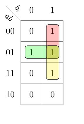
We see that the output signals are also mutually exclusive like the inputs.
This table can be drawn in a compact K-map in a variable-entered fashion:
|
|
|
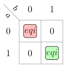

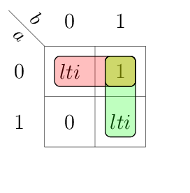
Above implicants result in the following Boolean equations.
Warning
Building the implicants in a variable-entered K-maps require more attention than a normal K-map. For details how to approach variable-entered K-maps, refer to page 3 of problem set 3 solutions.
In particular the 1s in the K-map for gto and lto must be expanded to gti | ~gti and lti | ~lti respectively. This leads to three minterms for each of the outputs gto and lto.
assign
eqo =
	(~a & ~b) | (a & b) & eqi
,
gto =
	(a & gti) | (~b & gti) | (a & ~b & ~gti)
,
lto =
	(~a & lti) | (b & lti) | (~a & b & ~lti)
;
Using these equations we can draw the circuit for a single bit-slice of the comparator.
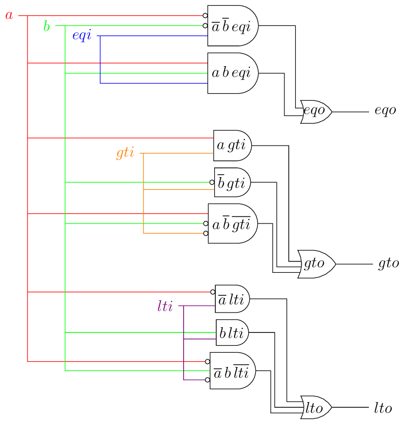
Fig. 7 Comparator single bit slice circuit diagram
Note
We could save some more transistors by double negating the and gate outputs. Doing this:
converts the
andgates tonandgates with some inverters at their inputsthe
orgates tonandgates.
2#
2a#
Modify the bit-slice block of problem 1 by removing the logic gates and signals that form the EQ output. Sketch a “block” circuit diagram for a 4-bit comparator that uses the modified bit slice blocks, and add a single gate to form the EQ output from the LT and GT outputs from the MSB (most significant bit).
We want to form the eq output using gt and lt in a 4 bit comparator.
If the numbers a and b are equal, then a is neither greater than nor less than b. In other words both gt and lt outputs of the last comparator must not be active. This corresponds to an 2 input and gate with all inputs negated or an 2 input nor gate:
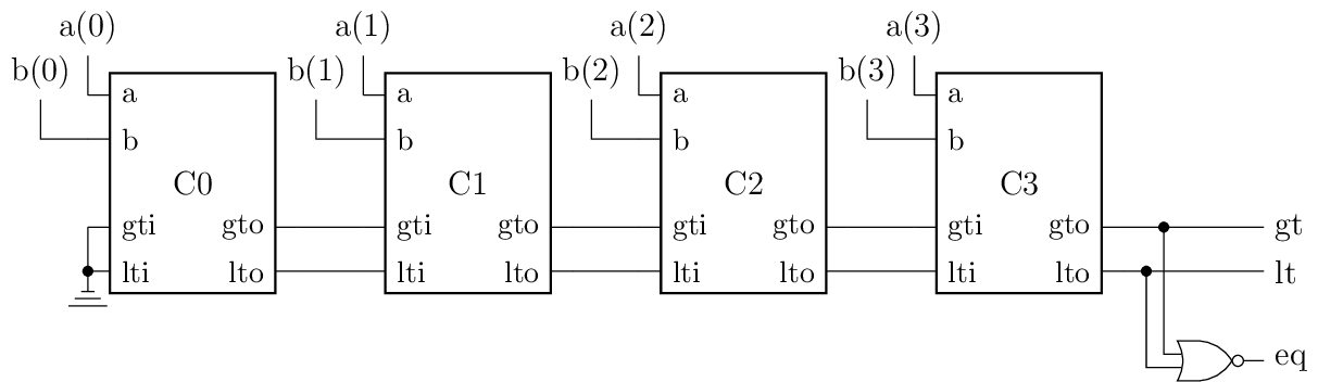
Fig. 8 Block diagram for a 4 bit comparator where ‘eq’ is formed using ‘lt’ and ‘gt’.
On a second thought we also should consider that gt and lt cannot be active at the same time. So it does not matter what the the circuit for eq should output in this case. In other words, this is a don’t care case. Let us draw the truth table:
|
|
|
|---|---|---|
0 |
0 |
1 |
0 |
1 |
0 |
1 |
0 |
0 |
1 |
1 |
dc |
We see that we can also form eq by using an XNOR gate. But using NOR consumes less transistors.
Now we have formed the eq output using the lt and gt outputs of the most significant bit slice. This saves the eq circuitry in the rest of the bit slices. The only disadvantage is that the eq output cannot be formed in parallel but has to wait for lt and gt outputs. This can make the circuit slower.
Note
This can make the circuit slower.
Why can but not will? Because it depends.
On one hand deriving an output from other outputs causes always an overhead on the critical path. We can overcome this by using parallel logic like we did in our first comparator implementation. On the other hand if the circuit becomes very large due to parallel logic (e.g., for the eq output), then additional logic must be placed further. This may lead to a longer critical path and thus slower circuit.
Last but not least, this exercise makes it clear that we could also have used the lt and gt outputs for forming the eq output which would save area for the single bit slice circuit. But in the multibit implementation using the lt and gt outputs of the most significant bitslice saves the most area.
2b#
Could you make the bit-slice modules even more efficient by leaving in the EQ logic and removing some other logic? Explain.
In previous problem we formed eq using gt and lt. We could also form:
gtusingeqandltltusingeqandgt
because all these outputs are mutually exclusive. If two of the signals is not active, then the third signal must be active. We can form the missing signal using a nor gate as we did in figure Block diagram for a 4 bit comparator where ‘eq’ is formed using ‘lt’ and ‘gt’..
So which output should we get rid of? Let us calculate the required area using figure Comparator single bit slice circuit diagram. We already did this kind of calculation in problem 9. Let us assume a nand gate implementation. The required transistor count for each output are:
eq: 2 inverters + 2x3inputnand+ 2inputnand\(= 4 + 12 + 4 = 20\)gt: 3 inverters + 2x2inputnand+ 2x3inputnand\(= 6 + 8 + 12 = 26\)lt: 3 inverters + 2x2inputnand+ 2x3inputnand\(= 6 + 8 + 12 = 26\)
So we could same more transistors by removing gt or lt instead of eq. But this can make the derived output gt or lt
3#
Complete truth tables and K-maps for HA and FA circuits, using XOR patterns where appropriate. Loop minimum SOP equations, and sketch the circuits (assume all inputs and outputs are active high).
3.1 Half adder#
|
|
|
|
|
|
3.2 Full adder#
|
|
|

|
|
|
4#
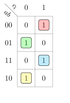
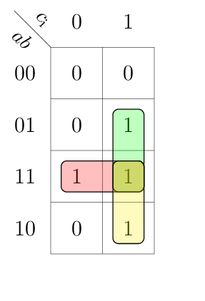
Sketch a block diagram for a full adder using two half-adder blocks and an OR gate.
A half adder can sum up three bits and a full adder three bits where the third bit is the \(c_\mathrm{i}\). If we cascade two half adders and
feed the output of one half adder to the second one
feed \(c_\mathrm{i}\) to the second half adder,
then we have the sum of three bits.
How can we form the carry out \(c_\mathrm{o}\) using only an additional or gate?
The carry output of the full adder is active if at least two of the three input bits are active. Which signals can we use to detect this? Maybe the carry output of the two half adders can help us. Let us analyze them.
The carry out of the first half adder \(c_{ab,\mathrm{o}}\) is active, if
aandbare active. (\(c_{ab,\mathrm{o}} = a \land b\))
The carry output of the second half adder \(c_{abci,\mathrm{o}}\) is high if
either \(a\) or \(b\) is active (results in \(s_{ab} = 1\))
and \(c_\mathrm{i}\) is active
which lead to \(c_{abci,\mathrm{o}} = a \lor b \land c_\mathrm{i} = a\, c_\mathrm{i} \lor b \, c_\mathrm{i}\).
Recall the three minterms from the previous problem for \(c_\mathrm{o}\):
\(c_\mathrm{o} = a\,b \lor b \, c_\mathrm{i} \lor a \, c_\mathrm{i}\)
We see that or-ing the two half adder carry outputs form \(c_\mathrm{o}\) of the full adder.
5#
Sketch an entire Carry-Propagate-Generate circuit that can form the carry-ins for all four bits of 5-bit CLA.
The carry-lookahead circuit inputs propagate (\(p\)) and generate(\(g\)) signals of each full adder and forms the carry input for the neighboring full adder by using a direct path. This approach leads to a faster circuit compared to a carry-ripple adder.
The problem asks for the carry-lookahead logic for a 5 bit adder. Let us say that the full adders are called \({F\!A}_0\) to \(F\!A_4\). Then the carry-lookahead logic for a 5 bit adder generates 4 carry signals \(c_1\) to \(c_4\), because \(c_0\) is an input to the carry-lookahead logic and \(c_5\) is an output of the adder.
Let us first begin with the equations. A carry input for a full adder is high, if
the previous full adder has a carry (generate)
or the previous full adder has (at least) one active input bit, so it will propagate the (generated or propagated) carry from the second previous full adder.
We can generate a fast path by expanding the previous carry outputs to avoid going through (in other words rippling) the previous full adders.
assign
c(1) = g(0) + ( p(0) & c(0) ),  # We cannot expand c(0)
c(2) = g(1) + ( p(1) & (
                        g(0) + ( p(0) & c(0) ) )
                       ),  # expanded c(1)
c(3) = g(2) + ( p(2) & (
                        g(1) + (
                                g(0) + ( p(0) & c(0) )
                               )
                       ),  # expanded c(2)
c(4) = g(3) + ( p(3) & (
                        g(2) + (
                                 g(1) + (
                                         g(0) + ( p(0) & c(0) )
                                        )
                                )
                       );  # expanded c(3)
TODO draw circuit
6#
Design a full-subtractor bit-slice circuit (Borrow-Ripple Subtractor). Label the inputs A, B, and Bin, and label the outputs D and Bout. Start by completing
the subtraction examples
complete the truth table and K-maps
sketch the circuit.
6.1 Subtraction examples#
|
|
|
|
|
|
|
|
The ellipsis (three dots) means that the neighboring number is repeated.
The rectangle in each of the subtraction examples show a single bit slice and the curved arrows depict the borrow-in and borrow-out signals.
Let us dive deeper in the second example from the first line to understand how borrowing works:
    1 0
    ↶ ↶
...0|0|1 0...
...1|1|0 0...
  -_______
   0|1|1 0
The most significant bit is 0, because there in two borrows. This results in the following values:
borrowing from the more significant bit \(2\)
borrow in from the less significant bit \(-1\)
the subtrahend of the current bit position \(-1\)
And thus to \(2-1-1=0\)
The complete examples follow:
|
|
|
|
|
|
|
|
6.2 Truth table and K-maps#
|
|
|
|
|
|
6.3 Circuit#
Because of the checkerboard pattern for \(d\) and the minterm 011 it seems difficult to combine the circuits for both outputs. The xor gate can be implemented with 10 transistors using two nor and one and gate (y = (~a&~b) ~| (a&b)) in CMOS and using 6 transistors if pass-gate-logic is used.
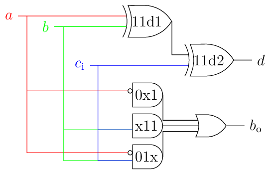
Instead of drawing a three leg xor gate two cascaded xors are drawn, because the word definition of exclusive or means that only one of the inputs must be active. This is a one-hot detector, but in our circuit the XOR gate counts the number of active input bits and outputs a one if the number is uneven. Refer to the section more than two inputs in Wikipedia about the XOR gate for the details.
Note
The library for drawing these diagrams also does not support drawing an XOR gate with more than two inputs. Frankly this behavior and the bugreport about this issue led me to this info.
7#
Complete the number conversions indicated. Note that all binary numbers are 8 bit two’s complement representations.
\(-19_d = \_\_\_\_\_\_\_\__b\)
\(1000\,0000_b = \_\_\_\_\_\_\_\__d\)
\(1001\,1010_b = \_\_\_\_\_\_\_\__d\)
\(-101_d = \_\_\_\_\_\_\_\__b\)
\(-19_d = 1110\,1101_b\)
\(1000\,0000_b = -1000\,0000 = -128_d\)
\(1001\,1010_b = -0110\,0110_b = -102_d\)
\(-101_d = -0110\,0101_d = 1001\,1011_b\)
8#
Complete the four 2’s compliment arithmetic problems below assuming that all operations use an adder. Showing both the decimal and binary numbers in each case.
8.1#
 17    0 0001 0001
-11  + 1 1111 0101
___  _____________
-22
+ 6  +
___  ______________
 35
-42  +
___  _______________
  19
-(-7)  +
_____  ______________
       1
 17    0 0001 0001
-11  + 1 1111 0101
___  _____________
   6    0 0000 0110
We have a carry out, but no overflow. An overflow happens if
two positive addends lead to a negative sum
two negative addends lead to a positive sum
because a negative and positive number can never overflow.
Note
This page about detecting overflow for two’s complement arithmetic from Thomas Bennet helped me to understand the importance of carry out and overflow. The pages also contain related examples.
So we can check an overflow by comparing the most significant bit of the two-complement numbers.
For the rest of the additions let us use as many bits as needed. For example \(-22\) needs the range \(-32\) to \(31\), so six bits are required.
-22    10 1010
+ 6  + 00 0110
___  _________
 -16   11 0000 (-01 0000)
No overflow, no carry out.
 35    010 0011
-42  + 101 0110
___  __________
 -7    111 1001 (-000 0111)
For \(-42\) and \(35\) seven bits are required. No overflow, no carry out.
  19     01 0011
-(-7)  + 00 0111
_____  _________
  26     01 1010
For \(19\) and \(-7\) six bits are required. No overflow, no carry out.
8.2#
Is the answer to the equation below correct in 8 bits? Explain.
         1010 0110
       + 1111 0101
_____  _____________
 1
  1010 0110 (-0101 1010) = -90
+ 1111 0101 (-0000 1011) = -11
_____________              ___
  1001 1011               -101
The answer is correct, because there is no overflow even there is a carry out. We already discussed the rules for an overflow above. Refer to this page for some two’s complement addition examples which lead to an incorrect sum.
Note
Some programming languages differentiate between unsigned and signed numbers. If these numbers would be unsigned numbers, then we would be adding \(166\) and \(245\). This would lead to an overflow and thus to a wrong sum.
In processors, an overflow is signaled by the overflow flag
9#
Sketch a circuit to convert a 4-bit binary number to its 2’s complement representation using only 3 XOR/XNOR gates and 2 AND or OR gates.
How can we create a circuit that generates two’s complement? We discussed in problem Exercise 147 what two’s complement means. In essence we subtract a \(n-1\) bit number from \(2^n\).
The problem asks for a circuit for a 4 bit number, so the 4 bit number would be the subtrahend and \(2^5\) would be our constant minuend. For example:
 1 0000
 0 1010 (-0110)
_______
 0 0110
It looks like we need a 5 bit subtractor, but in reality not. Unless the subtrahend is zero (which two’s complement is zero), the fifth bit of the difference will always be zero. So we only need a 4 bit subtractor.
We would place three full subtractors and one half subtractor for the least significant bit, because the carry-in is zero. \(b\) is the number that we want to convert to two’s complement and the \(a\) is the last four bits of \(2^n\) which are zero:
Let \(m\) be the minuend, \(s\) the subtrahend, \(d\) the difference and \(b\) the borrow. We discussed the equations for a subtractor in problem Exercise 148. These are:
Half subtractor:
assign
d = m ^ s,
b = ~m & s;
Full subtractor:
assign
d = m ^ s ^ b_in;
b_out = (~m & b_in) |
        (~m & s) |
        (s & b_in);
\(m\) is zero, so the equations can be simplified to:
Half subtractor:
assign
d = s,
b = s;
Full subtractor:
assign
d = s ^ b_in,
b_out = b_in |
        s |
        (s & b_in);
b_out can be further simplified because b_in | s includes s & b_in:
assign
d = s ^ b_in,
b_out = b_in | s;
So for a 4-bit circuit with \(s\) as input and \(d\) as output we get the following equations:
assign
d(0) = s(0),

b_in(1) = s(0),
d(1) = s(1) ^ s(0),

b_in(2) = s(0) | s(1),
d(2) = s(2) ^ (
               s(0) | s(1)
              ),

b_in(3) = s(0) | s(1) | s(2),
d(3) = s(3) ^ (
               s(0) | s(1) | s(2)
              );
We see that we need three XOR gates and two OR gates to form the \(d\) output.
10#
Examine several examples of addition overflow and subtraction underflow, and sketch a circuit below that can output a ‘1’ whenever an addition or subtraction result is incorrect due to underflow or overflow. Assume that both operands and result of the addition and subtraction are N-bits. (Hint: compare the carry in and carry out signals of the most-significant bit).
The result depends on whether we do signed or unsigned arithmetic.
Signed number arithmetic using two’s complement
Let us not differentiate between subtraction and addition and only analyze from the perspective from two’s complement addition which can also subtract.
Warning
Underflow in computer integer arithmetic referred to as integer overflow or integer wraparound. From Arithmetic underflow – Wikipedia:
Storing values that are too low in an integer variable (e.g., attempting to store −1 in an unsigned integer) is properly referred to as integer overflow, or more broadly, integer wraparound. The term underflow normally refers to floating point numbers only, which is a separate issue. …
In problem 8.1 we discussed that an overflow happens if:
two positive addends lead to a negative sum
two negative addends lead to a positive sum.
How can we implement a circuit that checks for these conditions? We could create a circuit which outputs a high value whenever these conditions apply, but the problem is that we have to calculate the most significant bit of the sum beforehand.
Is there another way to check for these conditions without calculating the sum? The first condition implies that in the most significant bit of the adder we get a 1 when the addend bits are zeroes. When does this happen? Let us analyze the carry-in and -out bits.
If the most significant addend bits …
are zeroes, we can only can get a
1if the carry-in signal is1. This will additionally lead to the carry-out being0. In summary:c_in & ~c_outare ones, we can only get a
0if the carry-in signal is0. This will additionally lead to the carry-out signal being1. In summary:~c_in & c_out
In the rest of the cases there should be no overflow. The conditions 1. and 2. correspond to overflow = c_in ^ c_out.
Let us check our hypothesis using some experiments:
|
|
|
|
Our experiments confirm our hypothesis.
Unsigned number addition
In case of unsigned numbers the most significant bit has a different meaning. In this case we have a overflow if the carry out signal of the most significant adder is 1.
Let us check our hypothesis using the same examples from signed number arithmetic and whether the results differ or not compared to the signed arithmetic:
|
|
|
|
The experiments confirm our hypothesis.
Unsigned number subtraction
Unsigned subtraction can be either done
using a subtractor circuit
by subtracting the subtrahend from \(2^n\) which corresponds to the two’s complement conversion
Note that even we use two’s complement conversion, the resulting numbers are not in two’s complement. In other words the most significant bit does not signify the sign of the number.
Refer to this Stackoverflow post for more details and example.
11#
Fill in the squares below to show all signal values when “1101” and “1010” are multiplied.
    b0 b1 b2 b3
    1  0  1  0
a0 1
a1 1
a2 0
a3 1
                    p13 p22  p03 p12 p21  p02 p11 p20  p01 p10  p00
                    0   0    0   1   0    1   0   0    0   1    1
           p23 p32          p31        p30
           0   1            0          1
      p33
      0
c_out
r7    r6   r5       r4       r3           r2            r1       r0  c_in
0     0    1        1        0            1             1        1   0