ADC reading#
An analog-to-digital converter is useful for digitizing an analog input coming from a peripheral device like a thermistor. For AD conversion we could use a peripheral chip that integrates an ADC but some FPGAs already integrate an ADC block, e.g., Intel MAX 10 or Xilinx 7 series FPGAs. The ADC block in 7 series FPGAs is called XADC.
In this tutorial we will use the XADC.
External Interface#
Xilinx already provides an application note for using the XADC. XADC has a reference voltage of 1V, but sensors may operate at higher voltages. For this purpose we can use a voltage divider. For example assume that we want to scale a 3.3V signal to 1V, then we have to divide by 33 and multiply by 10. In other words the ratio of the resistors should be 23 to 10. A circuit that uses standard resistor values looks like:
  --
  || 22k
 ---------
 || 10k || 220k
 ---------
Internal Interface#
Synthesizers cannot infer(instantiate automatically) hard blocks with a very special function[^ram_can_be_synthesized] like PCIe, clock manager or ADC from a behavioral description. So we have to instantiate the XADC manually.
Note
Synthesizers cannot instantiate hard blocks with a very special function
But memory components like RAM or DSPs can be inferred.
Every FPGA family has a library for components which are available for instantiation, for example 7 Series FPGA and Zynq-7000 SoC Libraries Guide (UG953) which also includes the XADC. In Design Entry Method section we see:
Instantiation Yes
Inference No
IP Catalog Recommended
…
This table confirms that the block cannot be inferred. The library recommends instantiating the block using the IP Catalog which you may find more convenient if you are mainly working with the Vivado GUI. Here we will focus on a manual instantiation.
The guide refers to the dedicated user guide for the XADC (UG480) which includes a section about instantiating the XADC.
Components#
According to the overview figure in section XADC Overview XADC block consists of a dynamic reconfiguration port (DRP), status and configuration registers, two ADCs and multiplexers which support one dedicated input and 16 additional configurable inputs.
Note
Dedicated means that this FPGA pin can only be connected to the ADC. In contrast, the configurable inputs can also be used as general input output.
Two separate ADC blocks allow simultaneous sampling of two channels TODO continue with excerpt
Configuration#
XADC does not only have many inputs but also many parameters that initialize the configuration registers. The Verilog instantiation example in UG480 already provides some example inputs, but to keep our template simple we will start with default parameters of the module.
Let us look at the default register values of the XADC found on the table Available Attributes in section XADC of the library guide and modify the registers that we need to have a minimal instantiation template.
We see that all register values are 0 with the exception of Configuration register 2 which is set to 16'h0800. The set bit corresponds to the clock division bit 3 (CD3). According to the DCLK division table in this configuration the DRP clock DCLK is divided by 8.
Note
DCLK is the only clock input to the module which is both used for the dynamic reconfiguration block and the ADC block.
Let us assume that we have a clock of 100 MHz. Can we leave it as a default value? To find out we can refer to the XADC specifications in the switching characteristics datasheet. On the table we see:
DRP clock frequency - DCLK - … – 8 – 250 MHz
ADC clock frequency - ADCCLK - Derived from DCLK – 1 – 26 MHz
So 100 MHz for DRP and \(100/8=12.5\,\mathrm{MHz}\) for ADCCLK should work and we can leave the default value.
Setting the ADC mode#
According to the chapter Sequencer Modes in UG480
… In [default mode], the XADC automatically monitors the on-chip sensors and stores the results in the status registers. Both ADCs are calibrated in this mode and an averaging of 16 samples is applied to all sensors. … The XADC also operates in default mode after initial power-up and during FPGA configuration … All alarm outputs (ALM[7:0]) except OT are disabled in default mode. ADC calibration is automatically enabled in default mode.
The 7 Series FPGAs have many on chip sensors that monitor the die temperature and supply voltages for various blocks. OT stands for over temperature is related to the die temperature. The alarm outputs are related to the supply voltages. An alarm output is active if the corresponding on chip sensor reach a preset threshold.
Note
Complex circuit blocks configuration and status are typically done using registers. Some status register bit are output as interface signals. ALM and OT are an example of this practice. These outputs can be found the flag register
In the sequencer mode the ADC measures a sequence of channels one after another. The measured channels according to the default mode sequence table include calibration of ADC and measurement of all on-chip sensors but not the external measurement pins V and VAUX
Simulation#
Section PC Board Design Guidelines in UG480 includes an example testbench which is helpful but rather unwieldy. We will create a more simple circuit and then build on that.
XADC converts analog voltages to digital values, so we have to feed the module with an analog signal. But using Systemverilog we can only describe the behavior of digital circuits. To overcome this limitation the simulation model of XADC supports reading a structured text file for the simulated voltages at the analog pins. The file is a space-separated and called design.txt as default. We will use the example provided in the user guide (in the section beginning with HDL example):
Note
Simulation of analog behavior VHDL and Verilog do not support description of analog behavior, but there are industry standards that overcome this limitation:
TIME   VAUXP[0] VAUXN[0] VAUXP[1] VAUXN[1] VAUXP[2] VAUXN[2] VAUXP[3] VAUXN[3] Temp VCCINT VCCAUX VCCBRAM
00000  0.005    0.0      0.200    0.0      0.50     0.0      0.1      0.0      25   1.00   1.80   1.00
34000  0.020    0.0      0.400    0.0      0.49     0.0      0.2      0.0      85   1.05   1.90   1.05
67000  0.049    0.0      0.600    0.0      0.51     0.0      0.5      0.0      20   0.95   1.71   0.95
99999  0.034    0.0      0.900    0.0      0.53     0.0      0.0      0.0      125  1.00   1.80   1.00
The column headers beginning with V are voltage inputs and Temp in the temperature in Celsius. Time is in ns. So time value of 10000 corresponds to 10 μs.
Now we continue with configuration of the design for instantiation.
Default mode#
In section Configuration we discovered the default mode which does not require any configuration. So let us prepare a testbench that only provides clock and reset to the circuit and check the behavior.
`timescale 1ns / 1ps
module xadc_default_behavior_tb;

logic clk = 0, rst;

XADC dut (
	.RESET(rst),
	.DCLK(clk)
);
always #1 clk = ~clk;

initial begin
	$dumpfile("signals.vcd");
	$dumpvars;

	rst = 1;
	#10 rst = 0;

	#100_000
	// At ~100 us temperature is set to 125. At the end of the next sequence
	// (not current sequence) latest the over-temperature signal should be
	// active.
	@(posedge dut.EOS);
	@(posedge dut.EOS);
	assert (dut.OT);
	$finish;
end
endmodule
SRC += $(XILINX_VIVADO)/data/verilog/src/glbl.v
SRC += $(XILINX_VIVADO)/data/verilog/src/unisims/XADC.v
include iverilog.mk
TIME   VAUXP[0] VAUXN[0] VAUXP[1] VAUXN[1] VAUXP[2] VAUXN[2] VAUXP[3] VAUXN[3] Temp VCCINT VCCAUX VCCBRAM
00000  0.005    0.0      0.200    0.0      0.50     0.0      0.1      0.0      25   1.00   1.80   1.00
34000  0.020    0.0      0.400    0.0      0.49     0.0      0.2      0.0      85   1.05   1.90   1.05
67000  0.049    0.0      0.600    0.0      0.51     0.0      0.5      0.0      20   0.95   1.71   0.95
99999  0.034    0.0      0.900    0.0      0.53     0.0      0.0      0.0      125  1.00   1.80   1.00
TOP ?= $(basename $(firstword $(wildcard *.v)))
SRC += $(lastword $(wildcard *.v))
# If only TOP.v and TOP_tb.v exist, firstword returns TOP_tb.v, lastword TOP.v. If only TOP.v exists, then both are the same file.

# LIB +=
# Library files added as -l$FILE

IVERILOG_OPTS ?= -g2012

#### End parameters ####
default: signals.vcd

SIM_MODEL = $(TOP)

SRC := $(sort $(TOP).v $(SRC))
# Remove duplicates in case $(TOP) and $(SRC) are the same file.

# Creates the model for simulation
$(SIM_MODEL): $(SRC) $(LIB)
	iverilog \
		$(IVERILOG_OPTS) \
		$(addprefix -l,$(LIB)) \
		-o $(TOP) \
		$(SRC)

# Executes the model
signals.vcd: $(SIM_MODEL)
	./$(TOP)

# Visualizes the signals
vis: signals.vcd
	gtkwave -A $<
# If signals.gtkw is provided as a Gtkwave save file, it will be read.

clean:
	rm -rf $(TOP)
	rm -f signals.vcd
Note
What happens if we leave a module port unconnected?
If we do not want to provide any input to a module port, we can leave the port unconnected like we did in
XADC dut (
	.RESET(rst),
	.DCLK(clk)
);
This behavior is described in the standard:
23.2.2.4 Default port values:
A module declaration may specify a default value for each singular input port. These default values shall be constant expressions evaluated in the scope of the module …
When the module is instantiated, input ports with default values can be omitted from the instantiation, and the compiler shall insert the corresponding default values. If a connection is not specified for an input port and the port does not have a default value, then, … the port shall either be left unconnected or result in an error …
23.3.3.3 Port connection rules for nets with built-in net types:
An input … If left unconnected, it shall have the value ‘z.
In summary, if there are no default values defined for a port and we do not explicitly connect this port, then it will have the value ‘z in the simulation.
Leaving an output unconnected is allowed too. This means that we do not want this output to have any effect on other signals.
Note
How do we access internal signals of a module in a testbench?
In Verilog we do not have to route internal signals to the module ports to probe them in the testbench. Instead we can use hierarchical signals as shown in xadc_default_behavior_tb.v:
@(posedge dut.EOS);
@(posedge dut.EOS);
assert (dut.OT);
According to the user guide the over temperature signal OT should be active if temperature rises to 125°C and the simulation confirms that:
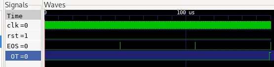
We observe that OT goes high after 100 μs. Now we will continue with the measurement of an external signal.
Measuring an external pin#
If we want to convert an external analog signal, then we have to apply a different configuration. The external pins that we can use are V pin and VAUX pins. We will use the V input in the following.
V input is a dedicated input for ADC conversion compared to VAUX pins. In other words, V pin is only designed for analog signals, but VAUX is multiplexed to a general purpose pin of the FPGA and thus be used also as a general purpose logic pin.
For configuration of the XADC the three configuration registers of the XADC are used. These registers can be directly preset using XADC module parameters instead of configuring them in runtime. These registers in turn consist of many configuration bits.
Providing the configuration using only numbers (in other words zeroes and ones) can lead to errors. A better practice is to define the register names and configuration bits using constants. As these constants can become lengthy we should better put them in a package file. Using a package has the additional benefit of importing these constants in another module when interacting with XADC. An excerpt of the package follows:
package xadc;
localparam
// Registers in dynamic reconfiguration port
DADDR_WIDTH = 7,
STAT_V = 7'h03,
CFG0 = 7'h40,
CFG1 = 7'h41,
CFG2 = 7'h42,

// CFG0
CAVG = 16'b1 << 15,  // Calibration averaging disable (fixed at 16 samples)

// Averaging
AVG1 = 16'b1 << 13,
AVG0 = 16'b1 << 12,
AVG_OFF = 16'b00 << 12,
AVG_16 = 16'b01 << 12,
AVG_64 = 16'b10 << 12,
AVG_256 = 16'b11 << 12,
We can use these names by overlaying them with the logical or operator.
Note
There are multiple ways to define constants in Systemverilog. These are defined in chapter 6.20:
Constants are named data objects that never change. SystemVerilog provides three elaboration-time constants:
parameter,localparam, andspecparam. SystemVerilog also provides a run-time constant,const…
parameter is used to create different versions of a module and can be set during instantiation. localparam is defined like parameters but cannot be changed. localparam may be based on parameter though.
An alternative way for defining constants is defining macros using the compiler directive `define (ch. 22.5.1) like in the programming language C. We should prefer the language constructs instead of macros, because language constructs can have a meaning in the language itself compared to a macro which is merely a substitution. Using localparams has the additional benefit of being one character shorter compared to constants defined by `define, e.g., STAT_V vs `STAT_V.
Refer to the article localparam in param port list by Eunchan Kim for the evolution of parameterizable ports in Verilog.
Now we can start with our module definition. We import these constants using import xadc::* and configure the following:
averaging over 16 values to filter noise
single channel mode on
Vinput
To read the measured value of V we have to interact with the DRP. The rules of this interaction (in other words protocol) is described in DRP Timing section. We need to use address, data output and some handshake signals. End of conversion EOC signal is useful for delaying or read request, because it does not make sense to request the conversion value before a measurement is finished.
To keep our module lightweight we directly forward the data out DO where the measurement value will be present and the data ready DRDY signal which signifies that data can be read. We forward them as v and v_vld which stands for valid.
The measured value will be a number from \(0\) to \(2^{16}-1\), which correspond to \(0\,V\) and \(1\,V\) respectively.
We test the design using an analog stimulus file for the V input:
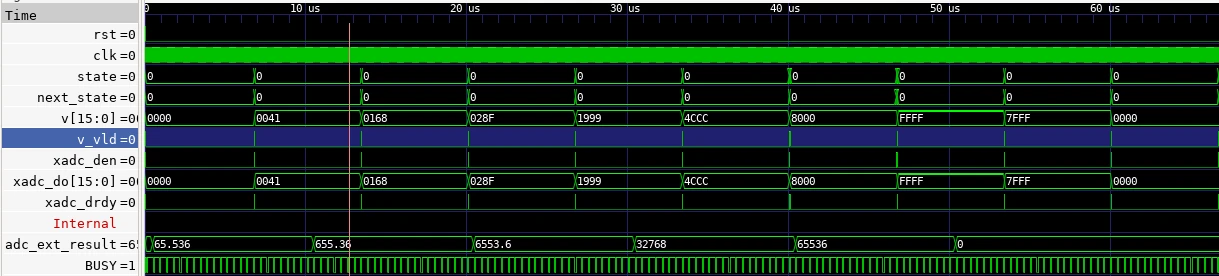
We observe that the our module outputs v and v_vld show the converted analog signals. We see more conversion values than specified in the analog stimulus file because XADC outputs an average of the last 16 values.
Implementation#
We will use the Boolean Board which has a 100 MHz clock and a potentiometer connected to the dedicated analog input V that consists of the pins VN and VP.
We test the circuit from section Measuring an external pin on the Boolean board by directly connecting v and v_vld to LEDs.
Note that we do not have to connect VN and VP ports neither on the XADC module nor in the constraints file. These are dedicated inputs connected to the specific pins on the chip package, so we do not have to constrain them.
Demo#
v_vld is connected to the green channel of the RGB LED0. This LED’s intensity is very low, because it is off for a long amount of time before it is activated again. In other words v_vld has a short duty cycle.
When we set the minimum voltage using the potentiometer we still observe that 8 LEDs are active instead of zero. 8 LEDs correspond to the voltage of roughly \(\frac{1\,V \cdot 2^9}{2^{16}} \approx 0.008\,V\) which is very low. Maybe this is related to some noise.
Project files#
import xadc::*;

module xadc_ext_pin_reading
#(
localparam RW = 16  // Register width
)(
input clk, rst,
output [RW-1:0] v,  // ADC reading for V pin
output v_vld
);

logic [RW-1:0] xadc_do;
logic
	xadc_den,
	xadc_drdy,
	xadc_eoc;
logic [DADDR_WIDTH-1:0] xadc_daddr = STAT_V;
// We could have provided STAT_V directly on the input port of XADC, but
// iverilog does not support this TODO bugreport

XADC #(
	.INIT_40(AVG_16 | CH_V),
	.INIT_41(SEQ_SNGL_CHNL)
	// CFG2 register: ADC clock DCLK/8 as default, no conf. needed
	)
	dut (
	.RESET(rst),
	.DCLK(clk),
	.DADDR(xadc_daddr),
	.DO(xadc_do),
	.DEN(xadc_den),
	.DRDY(xadc_drdy),
	.EOC(xadc_eoc)
);

enum {WAIT_FOR_CONVERSION, SEND_REQUEST, WAIT_FOR_DRDY, READ_V} state, next_state;

always_ff @(posedge clk, posedge rst)
	state <= rst ? state.first() : next_state;

always_comb begin
	next_state = state;
	xadc_den = 0;

	unique case (state)
	WAIT_FOR_CONVERSION:
		if (xadc_eoc)
			next_state = state.next();
	SEND_REQUEST:
		begin
		xadc_den = 1;
		next_state = state.next();
		end
	WAIT_FOR_DRDY:
		if (xadc_drdy)
			next_state = state.first();
	endcase
end

assign v = xadc_do;
assign v_vld = xadc_drdy;
endmodule
package xadc;
localparam
// Registers in dynamic reconfiguration port
DADDR_WIDTH = 7,
STAT_V = 7'h03,
CFG0 = 7'h40,
CFG1 = 7'h41,
CFG2 = 7'h42,

// CFG0
CAVG = 16'b1 << 15,  // Calibration averaging disable (fixed at 16 samples)

// Averaging
AVG1 = 16'b1 << 13,
AVG0 = 16'b1 << 12,
AVG_OFF = 16'b00 << 12,
AVG_16 = 16'b01 << 12,
AVG_64 = 16'b10 << 12,
AVG_256 = 16'b11 << 12,

MUX = 16'b1 << 11,  // Multiplexer enable
BU = 16'b1 << 10,  // Bipolar(1) unipolar(0)
EC = 16'b1 << 9,  // Event-driven(1) continuous(0) sampling
ACQ = 16'b1 << 8,  // Increase acquisition time in single channel mode

// Channel select in single channel and external mux mode
CH4 = 16'b1 << 4,
CH3 = 16'b1 << 3,
CH2 = 16'b1 << 2,
CH1 = 16'b1 << 1,
CH0 = 16'b1 << 0,

CH_TEMP = 16'b0_0000,
CH_VCCINT = 16'b0_0001,
CH_VCCAUX = 16'b0_0010,
CH_V = 16'b0_0011,
CH_VREFP = 16'b0_0100,
CH_VREFN = 16'b0_0101,
CH_VCCBRAM = 16'b0_0101,
//TODO remaining channels
CH_VAUX0 = 16'b1_0000,
CH_VAUX1 = 16'b1_0001,
CH_VAUX2 = 16'b1_0010,
CH_VAUX3 = 16'b1_0011,
CH_VAUX4 = 16'b1_0100,
CH_VAUX5 = 16'b1_0101,
CH_VAUX6 = 16'b1_0110,
CH_VAUX7 = 16'b1_0111,
CH_VAUX8 = 16'b1_1000,
CH_VAUX9 = 16'b1_1001,
CH_VAUX10 = 16'b1_1010,
CH_VAUX11 = 16'b1_1011,
CH_VAUX12 = 16'b1_1100,
CH_VAUX13 = 16'b1_1101,
CH_VAUX14 = 16'b1_1110,
CH_VAUX15 = 16'b1_1111,

// CFG1
// Sequencer operation
SEQ3 = 16'b1 << 15,
SEQ2 = 16'b1 << 14,
SEQ1 = 16'b1 << 13,
SEQ0 = 16'b1 << 12,

SEQ_DEFAULT = 16'b0000 << 12,
SEQ_SNGL_PASS = 16'b0001 << 12,
SEQ_CONTINUOUS = 16'b0010 << 12,
SEQ_SNGL_CHNL = 16'b0011 << 12,
SEQ_SIMULTANEOUS = 16'b01xx << 12,
SEQ_INDEPENDENT = 16'b10xx << 12,
SEQ_DEFAULT2 = 16'b11xx << 12,

// Alarm output disable
ALM6 = 16'b1 << 11,
ALM5 = 16'b1 << 10,
ALM4 = 16'b1 << 9,
ALM3 = 16'b1 << 8,
ALM2 = 16'b1 << 3,
ALM1 = 16'b1 << 2,
ALM0 = 16'b1 << 1,
OT = 16'b1,  // Over temperature alarm disable

// Calibration enables
CAL3 = 16'b1 << 7,
CAL2 = 16'b1 << 6,
CAL1 = 16'b1 << 5,
CAL0 = 16'b1 << 4,

CAL_ADC_OFFSET = 16'b01 << 4,
CAL_ADC_OFFSET_GAIN = 16'b10 << 4,
CAL_SUPPLY_SENS_OFFSET = 16'b01 << 6,
CAL_SUPPLY_SENS_OFFSET_GAIN = 16'b10 << 6,

// CFG2
// Clock divider 8 bits
// Better specified as 24 << CD0
CD = 8,
CD7 = 16'b1 << (CD+7),
CD6 = 16'b1 << (CD+6),
CD5 = 16'b1 << (CD+5),
CD4 = 16'b1 << (CD+4),
CD3 = 16'b1 << (CD+3),
CD2 = 16'b1 << (CD+2),
CD1 = 16'b1 << (CD+1),
CD0 = 16'b1 << (CD+0),

// Power down
PD1 = 16'b1 << 5,
PD0 = 16'b1 << 4,

PD_PWRD_UP = 16'b00 << 4,  // All powered up
PD_ADC_B = 16'b10 << 4,  // ADC-B powered down
PD_XADC = 16'b11 << 4;  // Entire XADC powered down
endpackage
# Set Bank 0 voltage
set_property CFGBVS VCCO [current_design]
# Configuration bank voltage select
set_property CONFIG_VOLTAGE 3.3 [current_design]
# These attributes help Vivado to spot for errors
# More info: https://support.xilinx.com/s/article/55660

set_property -dict {PACKAGE_PIN F14 IOSTANDARD LVCMOS33} [get_ports {clk}]

# Onboard button 0
set_property -dict {PACKAGE_PIN J2 IOSTANDARD LVCMOS33} [get_ports {rst}]

# Onboard LEDs
set_property -dict {PACKAGE_PIN G1 IOSTANDARD LVCMOS33} [get_ports {v[0]}]
set_property -dict {PACKAGE_PIN G2 IOSTANDARD LVCMOS33} [get_ports {v[1]}]
set_property -dict {PACKAGE_PIN F1 IOSTANDARD LVCMOS33} [get_ports {v[2]}]
set_property -dict {PACKAGE_PIN F2 IOSTANDARD LVCMOS33} [get_ports {v[3]}]
set_property -dict {PACKAGE_PIN E1 IOSTANDARD LVCMOS33} [get_ports {v[4]}]
set_property -dict {PACKAGE_PIN E2 IOSTANDARD LVCMOS33} [get_ports {v[5]}]
set_property -dict {PACKAGE_PIN E3 IOSTANDARD LVCMOS33} [get_ports {v[6]}]
set_property -dict {PACKAGE_PIN E5 IOSTANDARD LVCMOS33} [get_ports {v[7]}]
set_property -dict {PACKAGE_PIN E6 IOSTANDARD LVCMOS33} [get_ports {v[8]}]
set_property -dict {PACKAGE_PIN C3 IOSTANDARD LVCMOS33} [get_ports {v[9]}]
set_property -dict {PACKAGE_PIN B2 IOSTANDARD LVCMOS33} [get_ports {v[10]}]
set_property -dict {PACKAGE_PIN A2 IOSTANDARD LVCMOS33} [get_ports {v[11]}]
set_property -dict {PACKAGE_PIN B3 IOSTANDARD LVCMOS33} [get_ports {v[12]}]
set_property -dict {PACKAGE_PIN A3 IOSTANDARD LVCMOS33} [get_ports {v[13]}]
set_property -dict {PACKAGE_PIN B4 IOSTANDARD LVCMOS33} [get_ports {v[14]}]
set_property -dict {PACKAGE_PIN A4 IOSTANDARD LVCMOS33} [get_ports {v[15]}]

# Color LED 0
set_property -dict {PACKAGE_PIN V4 IOSTANDARD LVCMOS33} [get_ports {v_vld}];  # RGB0_G
`timescale 1ns / 1ps
`define RW 16  // Register width

module xadc_default_behavior_tb;

logic clk = 0, rst, v_vld;
logic [`RW-1:0] v;

xadc_ext_pin_reading dut (
	.rst,
	.clk,
	.v,
	.v_vld
);
always #1 clk = ~clk;

initial begin
	$dumpfile("signals.vcd");
	$dumpvars;

	rst = 1;
	#10 rst = 0;

	#120_000
	// At ~100 us temperature is set to 125. At the end of the next sequence
	// (not current sequence) latest the over-temperature signal should be
	// active.
	//@(posedge v_vld);
	//assert (dut.OT);
	$finish;
end
endmodule
TIME   VP      VN
00000  0.0001  0
10000  0.001   0
20000  0.01    0
30000  0.1     0
40000  0.5     0
50000  1.0     0
60000  0.0     0
SRC += $(XILINX_VIVADO)/data/verilog/src/glbl.v
SRC += $(XILINX_VIVADO)/data/verilog/src/unisims/XADC.v
SRC += xadc.v xadc_ext_pin_reading.v
include iverilog.mk

xadc_ext_pin_reading_tb: design.txt xadc.v
TOP ?= $(basename $(firstword $(wildcard *.v)))
SRC += $(lastword $(wildcard *.v))
# If only TOP.v and TOP_tb.v exist, firstword returns TOP_tb.v, lastword TOP.v. If only TOP.v exists, then both are the same file.

# LIB +=
# Library files added as -l$FILE

IVERILOG_OPTS ?= -g2012

#### End parameters ####
default: signals.vcd

SIM_MODEL = $(TOP)

SRC := $(sort $(TOP).v $(SRC))
# Remove duplicates in case $(TOP) and $(SRC) are the same file.

# Creates the model for simulation
$(SIM_MODEL): $(SRC) $(LIB)
	iverilog \
		$(IVERILOG_OPTS) \
		$(addprefix -l,$(LIB)) \
		-o $(TOP) \
		$(SRC)

# Executes the model
signals.vcd: $(SIM_MODEL)
	./$(TOP)

# Visualizes the signals
vis: signals.vcd
	gtkwave -A $<
# If signals.gtkw is provided as a Gtkwave save file, it will be read.

clean:
	rm -rf $(TOP)
	rm -f signals.vcd
SYN_TOP ?= $(basename $(lastword $(wildcard *.v)))
SRC += $(SYN_TOP).v
# If only TOP.v and TOP_tb.v exist, firstword returns TOP_tb.v, lastword TOP.v

DESIGN_FILES = \
	$(SRC) \
	$(DESIGN_CONSTRAINTS_FILE)

PART := xc7s50csga324-1
DESIGN_CONSTRAINTS_FILE ?= boolean.xdc
DESIGN_CONSTRAINTS_URL := \
	https://www.realdigital.org/downloads/8d5c167add28c014173edcf51db78bb9.txt

# Configuration end ###########################################################

BITSTREAM := $(SYN_TOP).bit

# Default goal
.PHONY: syn
syn: program

.PHONY: program
program: program.tcl $(BITSTREAM)
	vivado $(VIVADO_OPT) -source $<

.PHONY: bitstream
bitstream: $(BITSTREAM)

SYN_PROJ := syn-proj/syn.xpr
.PHONY: syn-proj
syn-proj: $(SYN_PROJ)

VIVADO_OPT := \
	-tempDir /tmp \
	-nojournal \
	-applog \
	-mode batch

$(SYN_PROJ): syn-proj.tcl
	vivado $(VIVADO_OPT) -source $<

syn-proj.tcl:
	@echo create_project -part $(PART) syn.xpr syn-proj   > $@
	@echo add_files {$(SRC)}                             >> $@
	@echo set_property file_type SystemVerilog [get_files {$(SRC)}] >> $@
	@echo add_files $(DESIGN_CONSTRAINTS_FILE)           >> $@
	@echo set_property top $(SYN_TOP) [current_fileset]  >> $@
	@echo exit >> $@

$(DESIGN_CONSTRAINTS_FILE):
	curl $(DESIGN_CONSTRAINTS_URL) > $@

$(BITSTREAM): \
	syn.tcl \
	$(DESIGN_FILES) \
	| $(SYN_PROJ)
	vivado $(VIVADO_OPT) -source $<

# Run synthesis
## based on
## https://docs.xilinx.com/r/en-US/ug892-vivado-design-flows-overview/Using-Non-Project-Mode-Tcl-Commands
## TODO create a non-project flow
syn.tcl:
	@echo open_project $(SYN_PROJ)                     > $@
	@echo synth_design                                >> $@
	@echo opt_design                                  >> $@
	@echo place_design                                >> $@
	@echo phys_opt_design                             >> $@
	@echo route_design                                >> $@
	@echo report_timing_summary                       >> $@
	@echo report_utilization                          >> $@
	@echo report_power                                >> $@
	@echo write_bitstream -force $(BITSTREAM)         >> $@

program.tcl:
	@echo open_hw_manager                                 > $@
	@echo connect_hw_server                              >> $@
	@echo open_hw_target                                 >> $@
	@echo current_hw_device                              >> $@
	@echo puts \"Selected device: [current_hw_device]\"  >> $@
	@echo set_property PROGRAM.FILE {$(BITSTREAM)} [current_hw_device] >> $@
	@echo program_hw_device                              >> $@
	@echo close_hw_manager                               >> $@

syn-clean:
# Does not clean .tcl files. They could have been modified by the user.
	$(RM) vivado*.log
	$(RM) -r syn-proj
	$(RM) $(BITSTREAM)

clean: syn-clean

syn-clean-all: syn-clean
# Additionally removes files potentially user-modified files
	$(RM) syn-proj.tcl syn.tcl program.tcl
	$(RM) $(DESIGN_CONSTRAINTS_FILE)

clean-all: syn-clean-all